
Research
Research aim
표면을 바꾸면 빛은 어떻게 달라질까?What changes when light meets a different surface?
유리창에 내 모습이 비치는 것은 빛의 일부가 표면에서 반사되기 때문입니다. 빛은 물질을 만나면 반사되거나, 통과하거나, 흡수됩니다. 이때 물질의 종류뿐 아니라 표면 구조의 크기와 모양도 빛의 거동을 바꿉니다.
빛의 파장에 가까운 작은 구조에서는 빛의 파동 성질이 중요해집니다. 구조를 설계하면 반사를 줄이거나 특정 파장을 선택할 수 있고, 불규칙한 구조가 만드는 복잡한 무늬는 물체를 식별하는 광학적 지문으로 활용할 수 있습니다.
A window reflects your face because some of the light bounces off its surface. When light meets a material, it can be reflected, transmitted or absorbed. The material matters, but so do the size and shape of its surface structures.
At dimensions close to the wavelength of light, wave effects become especially important. Designed structures can reduce reflections or select particular wavelengths. Irregular structures can create complex patterns that act as optical fingerprints for identifying objects.
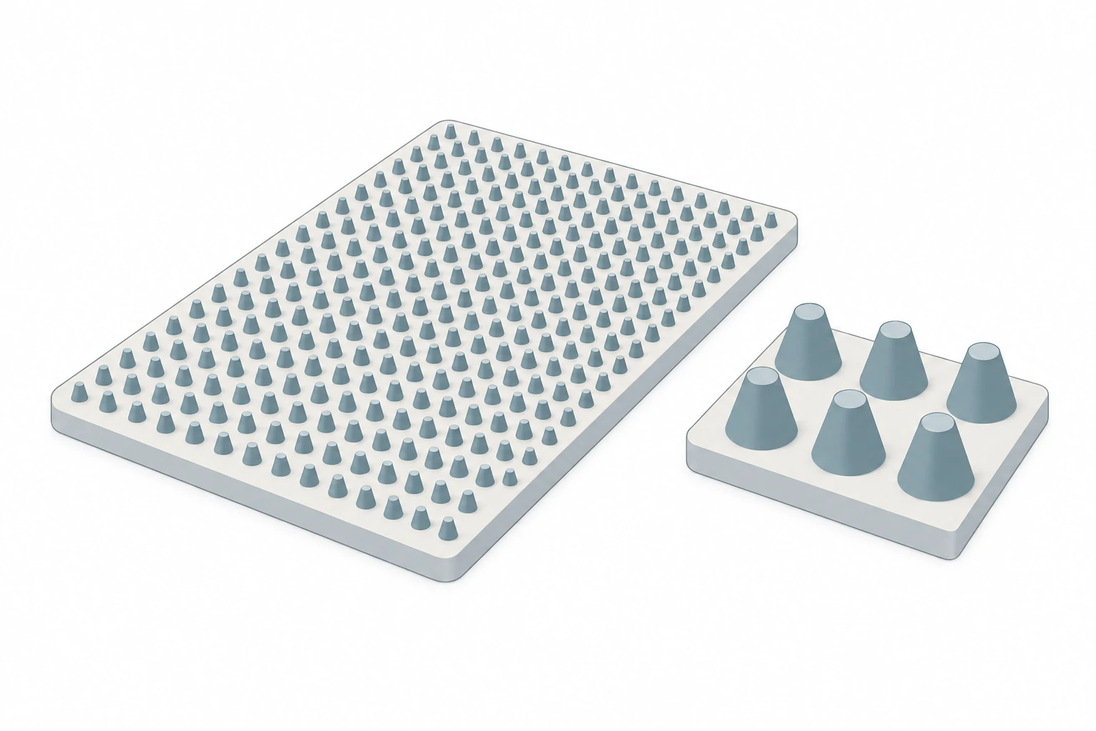
- 반사와 굴절Reflection & refraction
- 굴절률이 다른 물질의 경계에서 빛의 일부는 반사되고, 통과한 빛의 진행 방향은 달라질 수 있습니다.At a boundary between materials with different refractive indices, some light is reflected and transmitted light may change direction.
- 파장보다 작은 구조Subwavelength structures
- 파장보다 충분히 작은 표면 구조는 빛이 느끼는 유효 굴절률을 조절해 반사를 줄이는 데 쓰일 수 있습니다.Surface features much smaller than the wavelength can tailor the effective refractive index seen by light, helping reduce reflection.
- 회절과 간섭Diffraction & interference
- 미세한 틈을 지난 빛은 퍼지고 서로 겹칩니다. 구조가 달라지면 밝고 어두운 무늬도 달라집니다.Light spreads after passing through small gaps, and overlapping waves form bright and dark patterns that depend on the structure.
PIXEL에서 탐구하는 질문Questions we explore at PIXEL
이 분야에서는 나노구조의 모양과 배열을 실제 공정으로 구현하고, 광학 응답이 어떻게 달라지는지 살펴봅니다. 렌즈의 양면 반사를 줄이는 나노구조와 실크의 무작위 구조를 읽는 광학 PUF 연구는, 정밀한 설계와 자연스러운 불규칙성이 각각 어떻게 기능이 되는지 보여 줍니다. PUF는 구조마다 다른 물리적 응답을 인증에 이용하는 방식입니다.This area connects the shape and arrangement of nanostructures with fabrication and optical measurement. Published work on antireflection lenses and silk-based optical physical unclonable functions (PUFs) shows how both deliberate design and natural disorder can serve a purpose. A PUF uses the distinctive physical response of a structure for authentication.
함께 시작할 수 있는 연구Where you could begin
빛의 색, 재료의 표면, 반도체 공정에 관심이 있다면 이 분야를 탐색해 볼 수 있습니다. 구조를 바꿔 광학 응답을 예측하고, 현미경과 분광 측정 결과를 비교하는 과정에서 전자기학·재료·데이터 분석이 만납니다.If you are curious about colour, material surfaces or semiconductor processing, this is a place to explore. Predicting how a structure changes an optical response, then comparing microscopy and spectral measurements, brings together electromagnetism, materials and data analysis.
논문으로 만나는 연구Explore the research through our papers
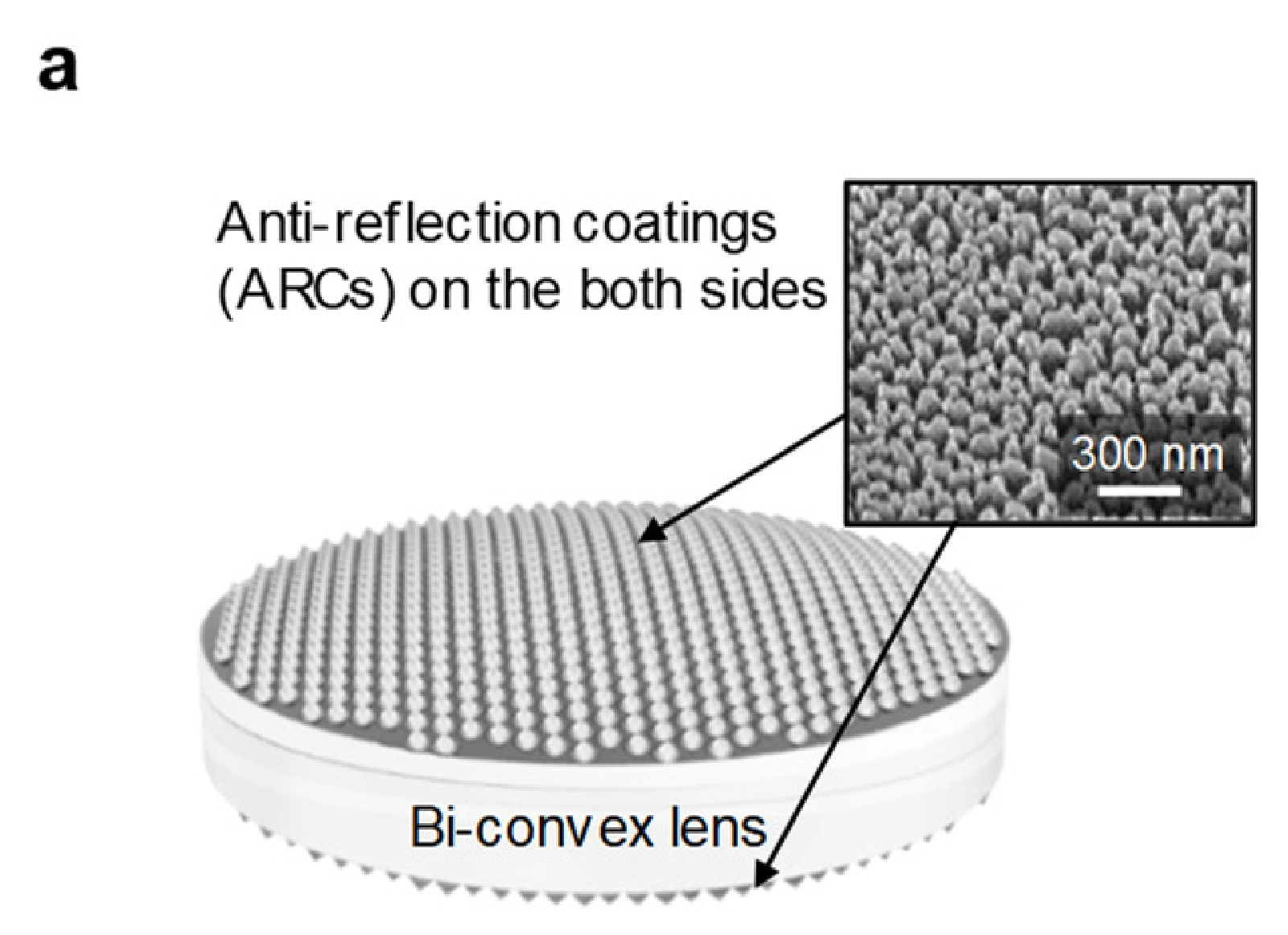
렌즈 양면의 반사를 줄이는 나노구조Nanostructures that reduce reflection on both sides of a lens
곡면 렌즈의 양쪽 면에 반사방지 나노구조를 형성했습니다. 평면에서 설계한 광학 기능을 실제 곡면 부품에 구현하는 공정의 중요성을 보여 줍니다.Antireflection nanostructures were formed on both sides of a curved lens, showing why fabrication on real optical surfaces matters as much as the design itself.
Coatings 9, 404 (2019)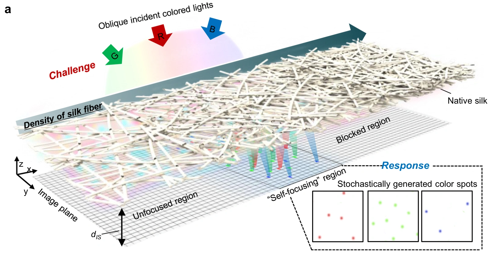
실크의 불규칙성을 광학적 지문으로Turning silk’s natural disorder into an optical fingerprint
천연 실크 섬유 사이의 무작위 틈이 만드는 광학 응답을 렌즈 없이 읽었습니다. 균일하게 만들기 어려운 미세구조를 인증에 활용한 사례입니다.The optical response from random gaps in native silk was read without a lens, turning naturally irregular microstructure into a resource for authentication.
Nature Communications 13, 247 (2022)작은 카메라로 더 넓고 선명하게 볼 수 있을까?How can a small camera see more?
카메라는 물체에서 온 빛을 렌즈로 모아 센서 위에 영상을 만듭니다. 더 넓은 장면을 담으려면 비스듬히 들어오는 빛까지 다뤄야 하고, 어두운 곳에서는 센서에 도달하는 적은 빛을 잘 활용해야 합니다. 픽셀 수를 늘리는 것만으로 해결하기 어려운 문제입니다.
렌즈의 모양과 조리개, 센서의 곡률과 흡수층은 모두 영상에 영향을 줍니다. 자연의 시각에서 발견한 설계 원리도 공학적인 렌즈와 반도체 센서로 옮길 수 있습니다. 핵심은 어떤 빛을 모으고, 어디에 초점을 맺으며, 얼마나 잘 검출하는지 함께 설계하는 것입니다.
A camera forms an image by gathering light from a scene onto a sensor. A wider view requires handling light arriving at oblique angles; a darker scene requires making good use of scarce light. More pixels alone cannot solve either problem.
The lens shape, aperture, sensor curvature and absorbing layers all influence the image. Principles found in natural vision can also be translated into engineered optics and semiconductor sensors. The central task is to design what light is collected, where it comes to focus and how well it is detected.
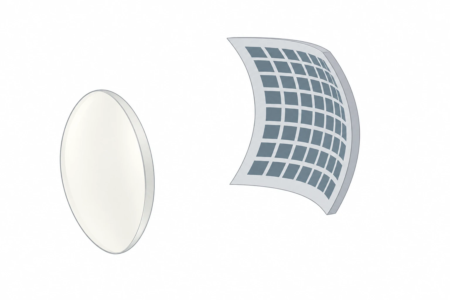
- 시야각Field of view
- 카메라가 한 번에 담는 장면의 각도입니다. 넓은 시야를 얻으려면 가장자리로 들어오는 빛도 고려해야 합니다.The angular extent of a scene captured in one image. A wide view requires careful handling of light from the edges of the scene.
- 초점과 센서 형상Focus & sensor geometry
- 렌즈가 선명한 상을 맺는 면은 반드시 평평하지 않습니다. 초점면과 센서의 형상을 맞추는 것도 설계 방법입니다.The surface on which a lens forms a sharp image is not always flat. Matching the sensor to that focal surface offers another design approach.
- 빛의 수집과 검출Light collection & detection
- 렌즈가 모은 빛도 센서에서 흡수되어야 신호가 됩니다. 흡수층과 반사층의 설계는 빛의 활용도를 바꿉니다.Collected light must be absorbed in the detector to produce a signal. Absorbing and reflective layers influence how effectively it is used.
PIXEL에서 탐구하는 질문Questions we explore at PIXEL
관련 연구에서는 렌즈와 센서를 하나의 이미징 시스템으로 다룹니다. 하나의 중심을 공유하는 구면 광학 구조인 단심 렌즈와 반구형 광다이오드 어레이를 결합해 넓은 시야를 구현했고, 다른 연구에서는 검출기 뒤의 반사층으로 빛을 다시 활용했습니다. 광학 설계가 센서 제작과 연결될 때 어떤 영상이 가능해지는지 탐구합니다.The related studies treat the lens and sensor as one imaging system. A monocentric lens, whose spherical optical surfaces share a common centre, was paired with a hemispherical photodiode array for wide-field imaging. Another study placed a reflector behind the detector to reuse transmitted light. Together, they connect optical design with the physical construction of an image sensor.
함께 시작할 수 있는 연구Where you could begin
카메라·로봇·영상 기술에 관심이 있다면, 광선 추적과 간단한 렌즈 실험부터 시작할 수 있습니다. 같은 장면이 렌즈와 센서 설계에 따라 어떻게 달라지는지 비교하며 기하광학, 소자 제작, 영상 분석을 연결해 볼 수 있습니다.An interest in cameras, robots or imaging can begin with ray tracing and simple lens experiments. Comparing the same scene across lens and sensor designs connects geometrical optics, device fabrication and image analysis.
논문으로 만나는 연구Explore the research through our papers
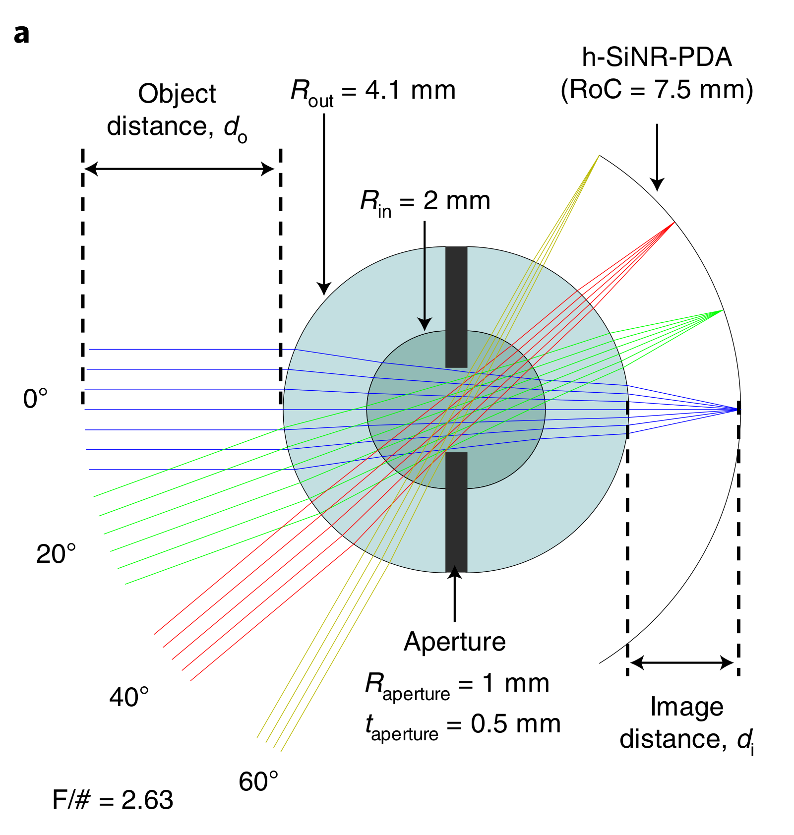
곡면 센서와 렌즈를 함께 설계한 광시야 카메라A wide-view camera built around a curved sensor
단심 렌즈와 반구형 실리콘 나노막대 광다이오드 어레이를 결합했습니다. 렌즈의 초점면에 맞춘 센서 형상으로 넓은 시야를 구현한 연구입니다.A monocentric lens was combined with a hemispherical silicon-nanorod photodiode array, demonstrating wide-field imaging by matching sensor geometry to the lens’s focal surface.
Nature Electronics 3, 546–553 (2020)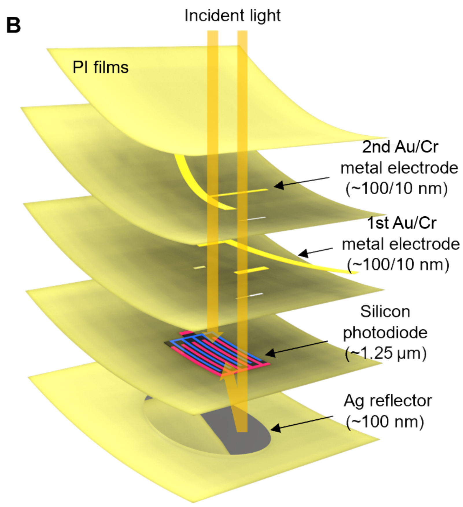
반사층으로 빛을 다시 활용하는 인공 시각Artificial vision that gives light another pass
광검출기 뒤에 은 반사층을 두어 통과한 빛이 다시 검출층을 지나도록 했습니다. 다양한 조명에서 물체를 구별하기 위한 인공 시각 시스템에 이 원리를 적용했습니다.A silver reflector behind the photodetector returns transmitted light through the detecting layer. This principle was incorporated into an artificial vision system for distinguishing objects under diverse lighting.
Science Advances 10, eadp2809 (2024)빛을 읽는 소자에 어떤 기능을 더할 수 있을까?What else can a light sensor do?
이미지 센서와 광학 웨어러블 기기의 출발점은 빛을 전기 신호로 바꾸는 반도체입니다. 흡수된 빛이 전하를 만들고, 소자 내부의 전기장이 그 전하를 이동시킵니다. 어떤 재료와 구조를 쓰느냐에 따라 검출할 수 있는 빛과 신호의 크기가 달라집니다.
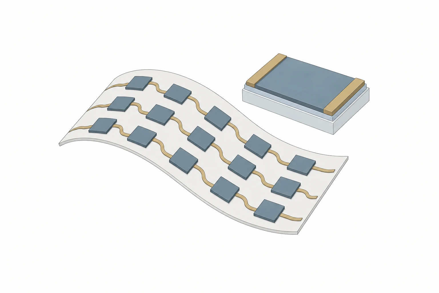
여기에 기능을 더할 수 있습니다. 소자의 전도 상태를 기억하고 조절하면 센서 안에서 신호를 처리할 수 있고, 얇은 소자와 유연한 배선을 결합하면 곡면에도 놓을 수 있습니다. 재료, 회로, 기계적 구조를 함께 설계하는 이유입니다.
Image sensors and optical wearables begin with a semiconductor that converts light into an electrical signal. Absorbed light generates charge, and electric fields inside the device move that charge. Materials and device structures determine which light can be detected and the resulting signal.
A sensing device can do more. Retaining and adjusting its conductive state can enable signal processing within the sensor. Combining thin devices with flexible interconnects can let them fit curved surfaces. Both directions call for materials, circuits and mechanical structures to be designed together.
- 광전 변환Photoelectric conversion
- 반도체가 흡수한 빛은 이동 가능한 전하를 만들 수 있습니다. 이 전하를 모아 빛의 세기를 전기적으로 읽습니다.Light absorbed by a semiconductor can generate mobile charge. Collecting this charge allows light intensity to be read electrically.
- 게이트와 기억Gating & memory
- 게이트 전압은 트랜지스터의 전류를 조절합니다. 분극이나 포획된 전하가 남는 구조에서는 이전 입력의 흔적을 유지할 수 있습니다.A gate voltage controls transistor current. Structures that retain polarization or trapped charge can preserve a trace of earlier inputs.
- 유연한 구조Flexible structures
- 얇은 소자와 휘어지는 배선은 굽힘에 따른 변형을 줄이거나 분산합니다. 전기적 성능과 기계적 안정성을 함께 살펴야 합니다.Thin devices and bendable interconnects can reduce or redistribute strain during bending. Electrical performance and mechanical stability must be considered together.
PIXEL에서 탐구하는 질문Questions we explore at PIXEL
관련 연구는 빛을 읽는 개별 소자에서 실제 센서 시스템까지 이어집니다. 강유전체 게이트 광트랜지스터에서는 빛으로 기록한 전도 상태를 전기적으로 조절해 센서 내부의 영상 처리를 탐구했습니다. 무선 조직 산소계에서는 광센서, 유연한 패치, 무선 전력과 복사 냉각을 결합해 착용 환경까지 고려했습니다.The related work spans individual sensing devices and integrated systems. Ferroelectric-gated phototransistors were used to electrically adjust optically recorded conductance for in-sensor image processing. A wireless tissue oximeter combined optical sensing, a flexible patch, wireless power and radiative cooling to address the conditions in which a wearable operates.
함께 시작할 수 있는 연구Where you could begin
반도체 소자, 회로, 웨어러블 기술이 궁금하다면 빛을 비추며 전류의 변화를 측정하는 실험부터 접근할 수 있습니다. 소자 특성 분석과 간단한 회로·데이터 처리를 연결하면 재료의 변화가 시스템 기능으로 이어지는 과정을 볼 수 있습니다.If semiconductor devices, circuits or wearables interest you, a starting point is measuring how current changes under illumination. Connecting device characterization with simple circuits and data processing reveals how material behaviour becomes a system function.
논문으로 만나는 연구Explore the research through our papers
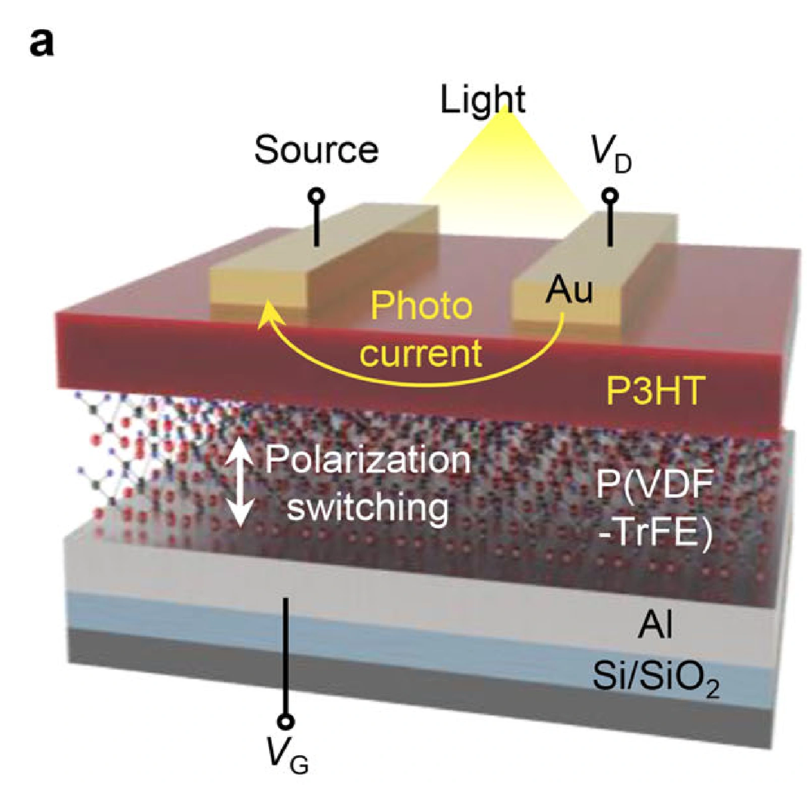
빛의 정보를 기억하고 조절하는 광트랜지스터A phototransistor that retains and adjusts optical information
빛으로 기록한 전도 상태를 강유전체 게이트로 조절했습니다. 조명이 달라져도 영상 정보를 적절한 범위로 보정하는 센서 내부 처리의 가능성을 보여 줍니다.A ferroelectric gate adjusts an optically recorded conductive state, demonstrating a route to recalibrating visual information within the sensor as illumination changes.
Advanced Materials 38, e03475 (2026)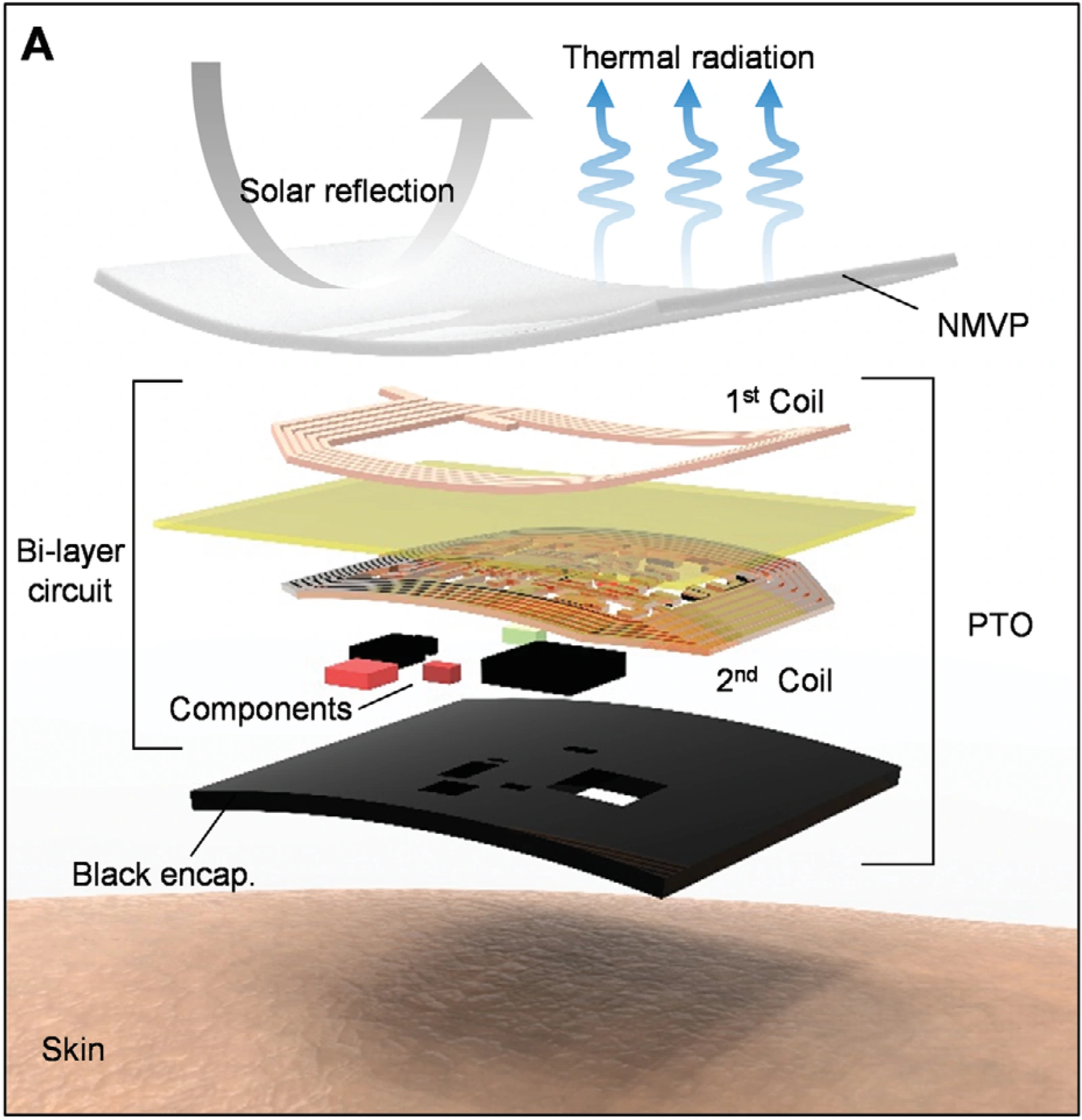
열 관리까지 고려한 무선 조직 산소계A wireless tissue oximeter with thermal management
두 파장의 근적외선으로 조직의 산소화 상태를 읽는 패치에 무선 전력과 복사 냉각을 결합했습니다. 센서의 성능뿐 아니라 야외 사용 시의 열 환경까지 함께 설계한 사례입니다.A patch that probes tissue oxygenation with two near-infrared wavelengths combines wireless power and radiative cooling, showing how sensor design extends to the thermal demands of outdoor use.
Advanced Science 8, 2004885 (2021)