표면을 바꾸면 빛은 어떻게 달라질까?What changes when light meets a different surface?
유리창에 내 모습이 비치는 것은 빛의 일부가 표면에서 반사되기 때문입니다. 빛은 물질을 만나면 반사되거나, 통과하거나, 흡수됩니다. 이때 물질의 종류뿐 아니라 표면 구조의 크기와 모양도 빛의 거동을 바꿉니다.
빛의 파장에 가까운 작은 구조에서는 빛의 파동 성질이 중요해집니다. 구조를 설계하면 반사를 줄이거나 특정 파장을 선택할 수 있고, 불규칙한 구조가 만드는 복잡한 무늬는 물체를 식별하는 광학적 지문으로 활용할 수 있습니다.
A window reflects your face because some of the light bounces off its surface. When light meets a material, it can be reflected, transmitted or absorbed. The material matters, but so do the size and shape of its surface structures.
At dimensions close to the wavelength of light, wave effects become especially important. Designed structures can reduce reflections or select particular wavelengths. Irregular structures can create complex patterns that act as optical fingerprints for identifying objects.
- 반사와 굴절Reflection & refraction
- 굴절률이 다른 물질의 경계에서 빛의 일부는 반사되고, 통과한 빛의 진행 방향은 달라질 수 있습니다.At a boundary between materials with different refractive indices, some light is reflected and transmitted light may change direction.
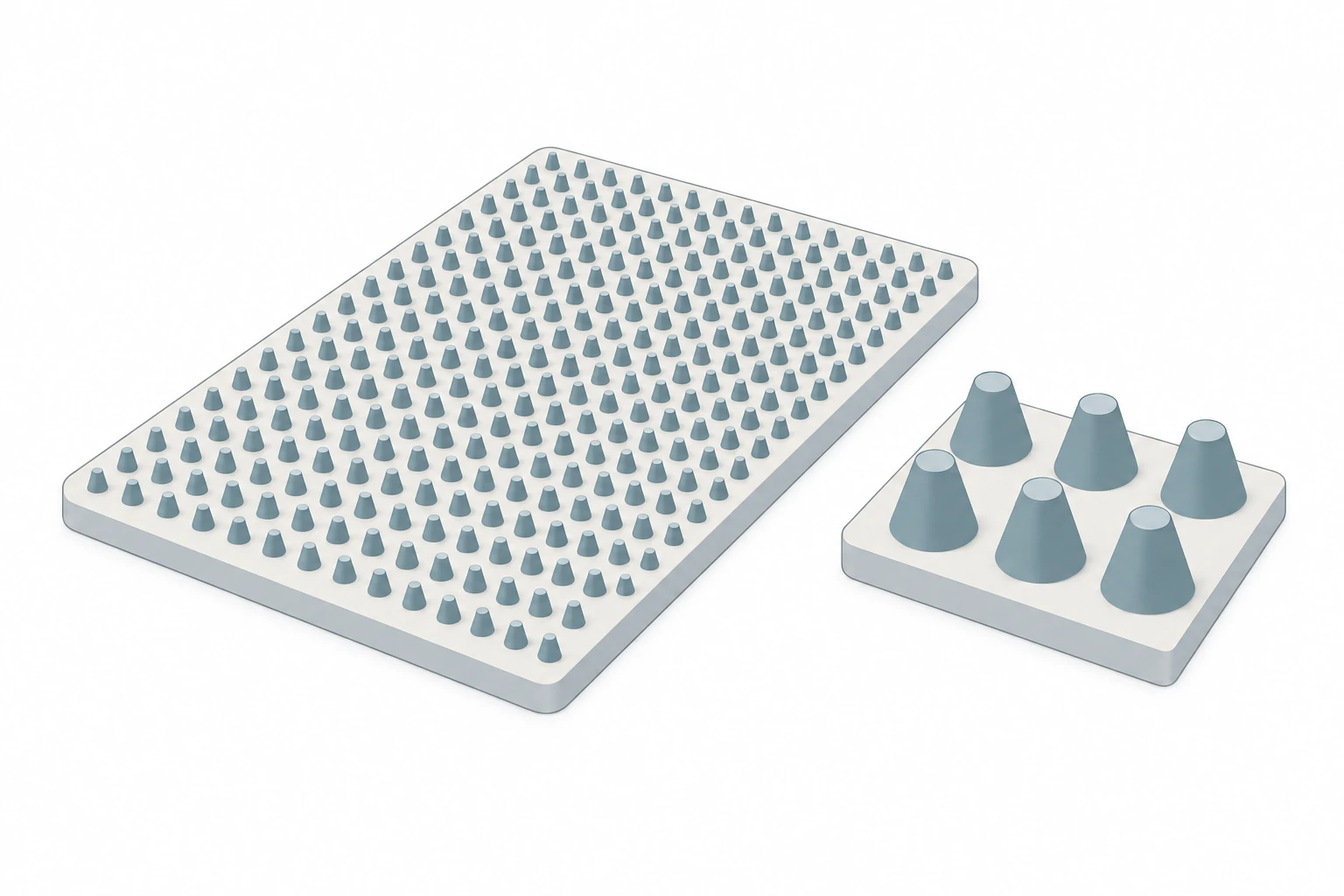
- 파장보다 작은 구조Subwavelength structures
- 파장보다 충분히 작은 표면 구조는 빛이 느끼는 유효 굴절률을 조절해 반사를 줄이는 데 쓰일 수 있습니다.Surface features much smaller than the wavelength can tailor the effective refractive index seen by light, helping reduce reflection.
- 회절과 간섭Diffraction & interference
- 미세한 틈을 지난 빛은 퍼지고 서로 겹칩니다. 구조가 달라지면 밝고 어두운 무늬도 달라집니다.Light spreads after passing through small gaps, and overlapping waves form bright and dark patterns that depend on the structure.
PIXEL에서 탐구하는 질문Questions we explore at PIXEL
이 분야에서는 나노구조의 모양과 배열을 실제 공정으로 구현하고, 광학 응답이 어떻게 달라지는지 살펴봅니다. 렌즈의 양면 반사를 줄이는 나노구조와 실크의 무작위 구조를 읽는 광학 PUF 연구는, 정밀한 설계와 자연스러운 불규칙성이 각각 어떻게 기능이 되는지 보여 줍니다. PUF는 구조마다 다른 물리적 응답을 인증에 이용하는 방식입니다.This area connects the shape and arrangement of nanostructures with fabrication and optical measurement. Published work on antireflection lenses and silk-based optical physical unclonable functions (PUFs) shows how both deliberate design and natural disorder can serve a purpose. A PUF uses the distinctive physical response of a structure for authentication.
함께 시작할 수 있는 연구Where you could begin
빛의 색, 재료의 표면, 반도체 공정에 관심이 있다면 이 분야를 탐색해 볼 수 있습니다. 구조를 바꿔 광학 응답을 예측하고, 현미경과 분광 측정 결과를 비교하는 과정에서 전자기학·재료·데이터 분석이 만납니다.If you are curious about colour, material surfaces or semiconductor processing, this is a place to explore. Predicting how a structure changes an optical response, then comparing microscopy and spectral measurements, brings together electromagnetism, materials and data analysis.
논문으로 만나는 연구Explore the research through our papers
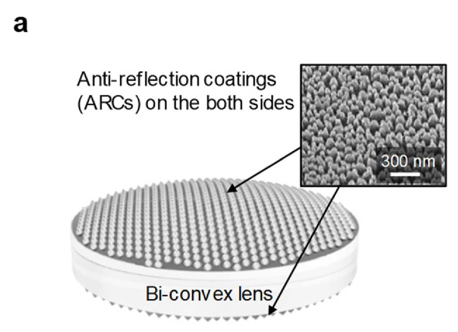
렌즈 양면의 반사를 줄이는 나노구조Nanostructures that reduce reflection on both sides of a lens
곡면 렌즈의 양쪽 면에 반사방지 나노구조를 형성했습니다. 평면에서 설계한 광학 기능을 실제 곡면 부품에 구현하는 공정의 중요성을 보여 줍니다.Antireflection nanostructures were formed on both sides of a curved lens, showing why fabrication on real optical surfaces matters as much as the design itself.
Coatings 9, 404 (2019)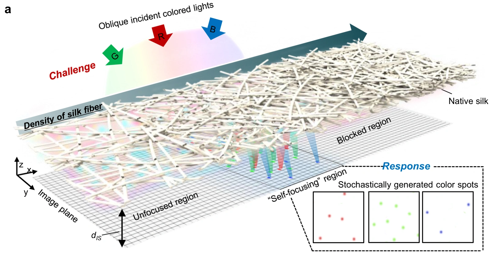
실크의 불규칙성을 광학적 지문으로Turning silk’s natural disorder into an optical fingerprint
천연 실크 섬유 사이의 무작위 틈이 만드는 광학 응답을 렌즈 없이 읽었습니다. 균일하게 만들기 어려운 미세구조를 인증에 활용한 사례입니다.The optical response from random gaps in native silk was read without a lens, turning naturally irregular microstructure into a resource for authentication.
Nature Communications 13, 247 (2022)Related publications
-
Hydrogel Thermostat Inspired by Photoprotective Foliage Using Latent and Radiative Heat Control
Advanced Materials 38(17), 2516537 (2026) (link)
-
Flexible infrared camouflage eutectic gallium-indium for thermoelectric energy harvesting
Nature Communications 17, 7684 (2026) (link)
-
ACS Nano 19(30), 27033-27074 (2025) (link)
-
Advanced Transparent Radiative Coolers: Materials, Design, and Applications
IEEE Journal of Selected Topics in Quantum Electronics 31(6), 9900114 (2025) (link)
Co-corresponding author
-
Advanced Materials 37(39), 2504288 (2025) (link)
-
ACS Applied Materials & Interfaces 14(39), 44419-44428 (2022) (link)
-
Advanced Materials 34(21), 2110003 (2022) (link)
-
Advanced Optical Materials 10(6), 2102388 (2022) (link)
-
Revisiting silk: a lens-free optical physical unclonable function
Nature Communications 13(1), 247 (2022) (link)
Co-first author
-
A Janus emitter for passive heat release from enclosures
Science Advances 6(36), eabb1906 (2020) (link)
-
Advanced Optical Materials 8(17), 2000198 (2020) (link)
-
Nature Communications 11(1), 328 (2020) (link)
-
ACS Applied Materials & Interfaces 11(39), 36020-36026 (2019) (link)
-
Double-sided anti-reflection nanostructures on optical convex lenses for imaging applications
Coatings 9(6), 404 (2019) (link)